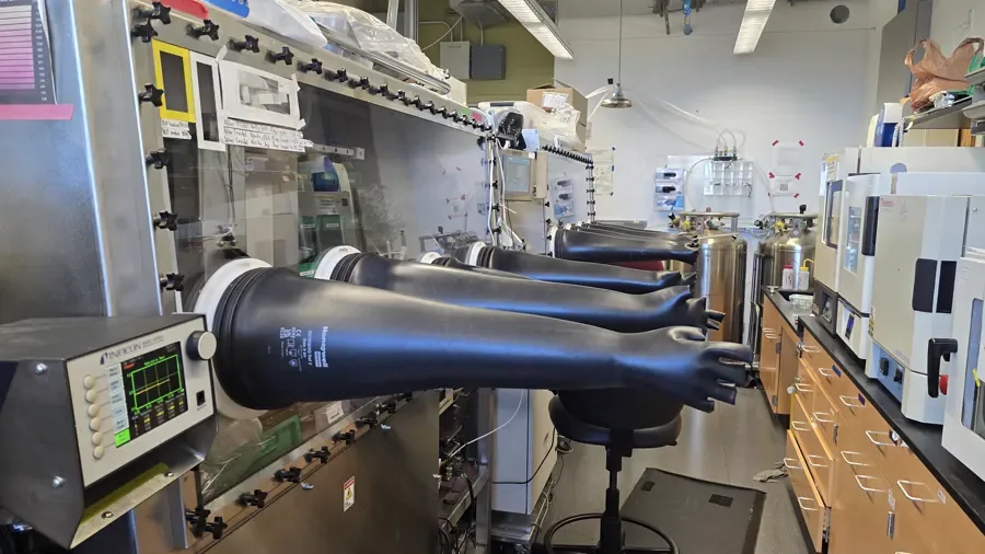
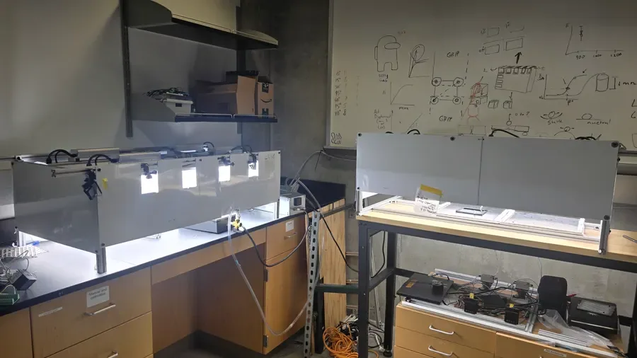
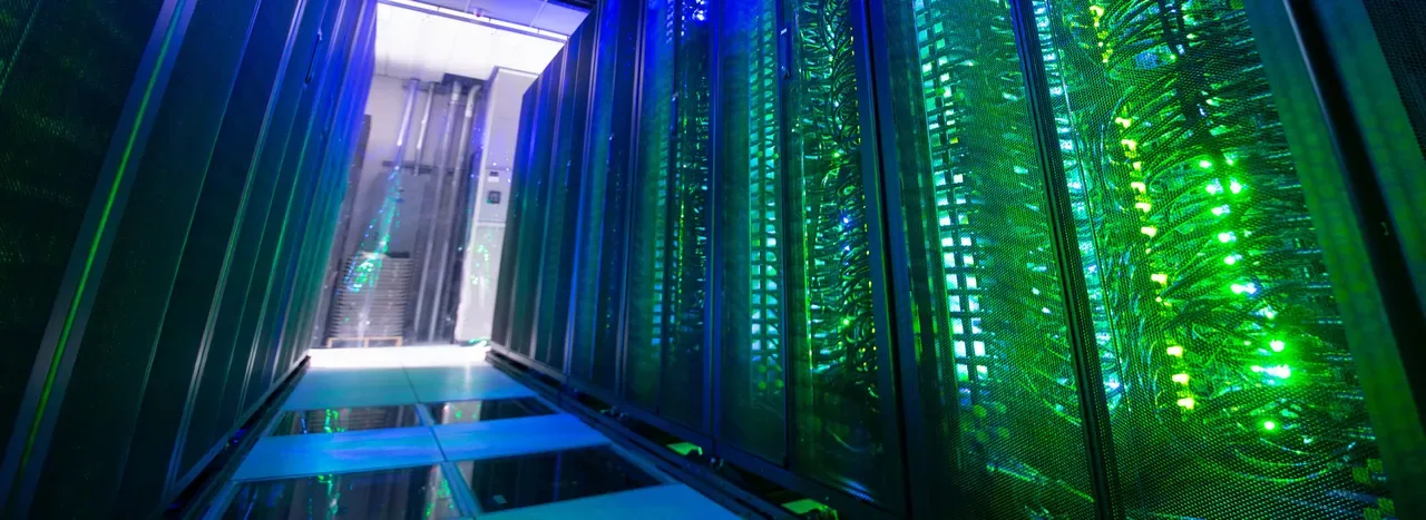
Solar-cell characterization equipment in the Fenning Research Group laboratory

Facilities

Automated Synthesis

Integrated tools for materials synthesis, processing, and characterization

Our lab combines automated perovskite processing, thin-film fabrication, electrochemistry, and advanced materials characterization.

PASCAL

Perovskite Automated Spin Coat Assembly Line

  • Two-Step Spin-Coating
  • Computer-Vision Assisted Pick and Place
  • Characterization Line

MEITNER

Meniscus Integration for Thin film Nano Electronics Robot

  • Ambient Compatible Computer-Vision Assisted Meniscus Coating
  • 6-Axis Robot Arm For Pick and Place
  • Translating Lab Scale Recipes to Large Area

Station 1 of 2: PASCAL

In-lab capabilities
Selected equipment

A representative look at the systems supporting photovoltaic, catalysis, and materials research in the group.
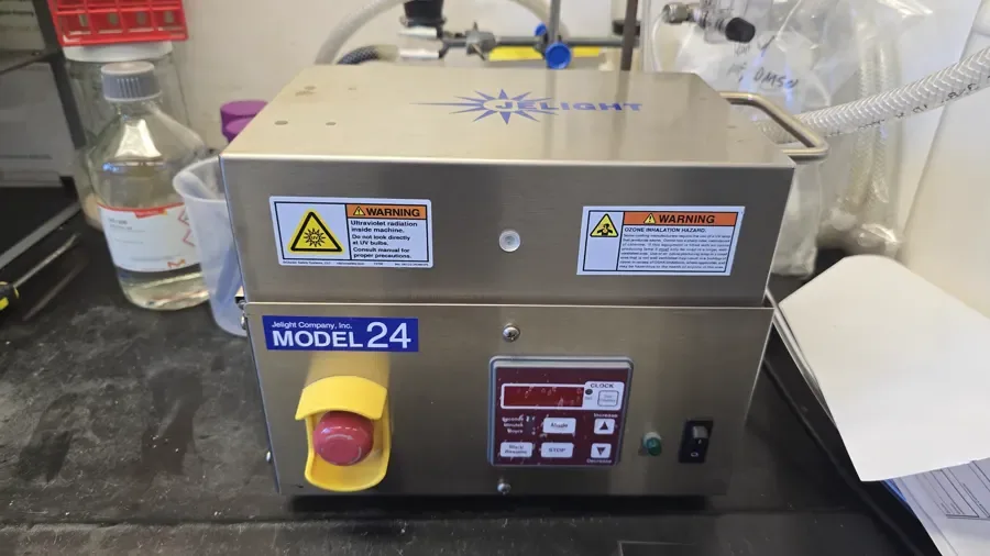
UV ozone surface treatment system

UV ozone treatment

Surface cleaning and preparation before thin-film deposition and device fabrication.
Physical vapor deposition system

Physical vapor deposition

Controlled thin-film deposition for contacts, interfaces, and device stacks.
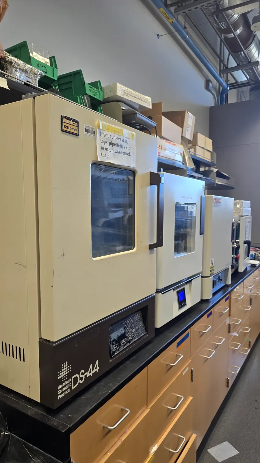
Laboratory thermal processing ovens

Thermal processing

Dedicated ovens for controlled annealing and materials processing.
Accelerated environmental stress testing equipment

Accelerated stress testing

Environmental aging and stability studies for materials and photovoltaic devices.
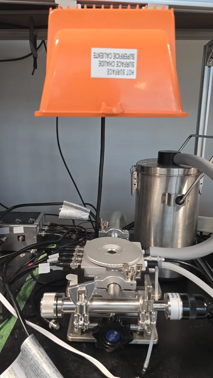
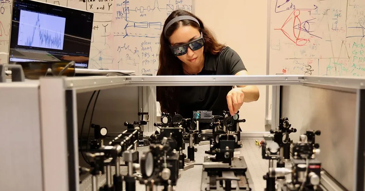
Optical cryostat and measurement setup

Cryogenic measurements

Temperature-dependent optical and electronic characterization.
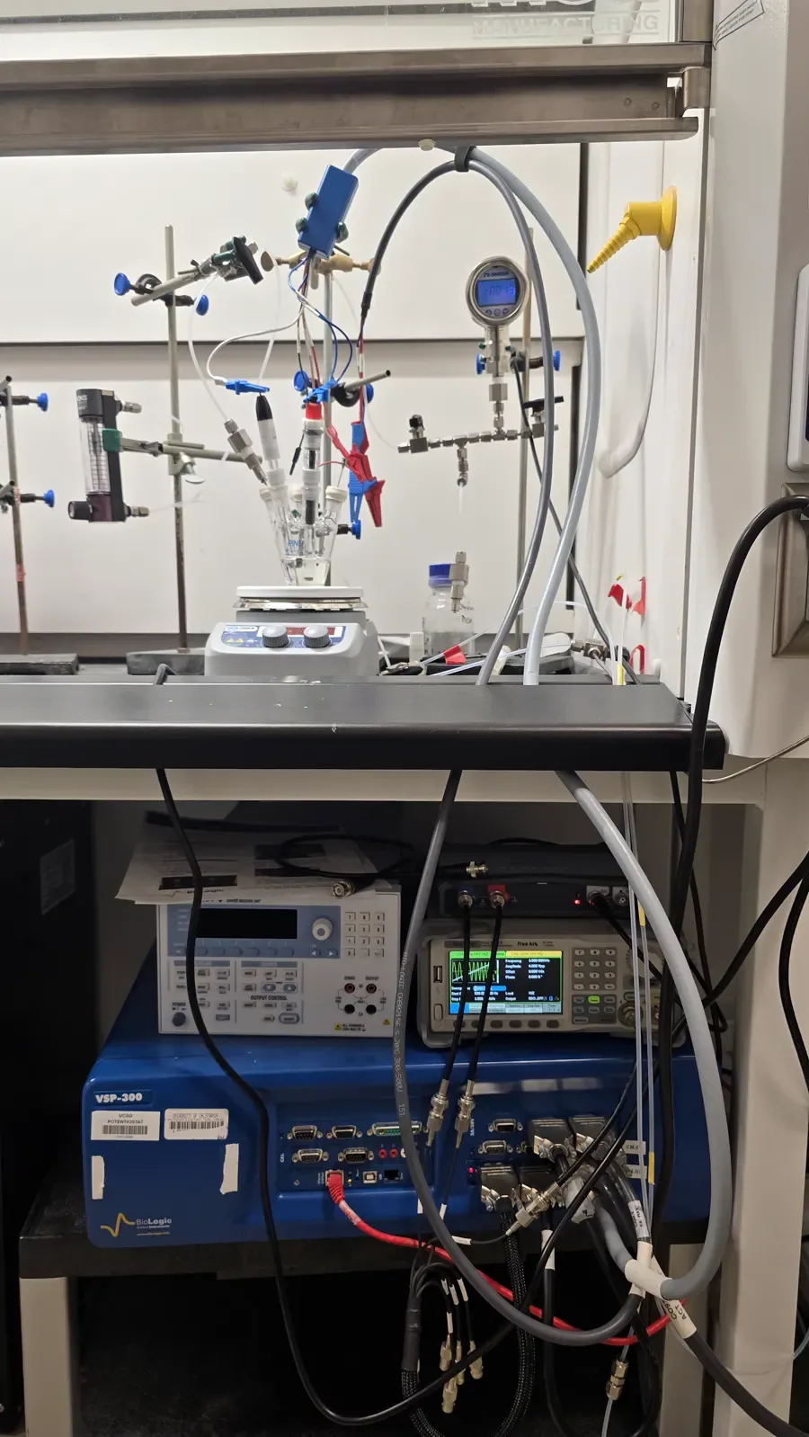
Electrochemistry workstation

Electrochemistry

Electrochemical testing for catalysis, solar fuels, and interface studies.
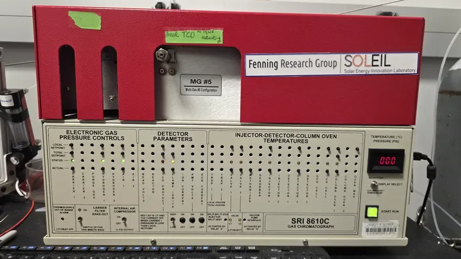
Gas chromatograph

Gas chromatography

Product separation and analysis for catalytic reaction studies.
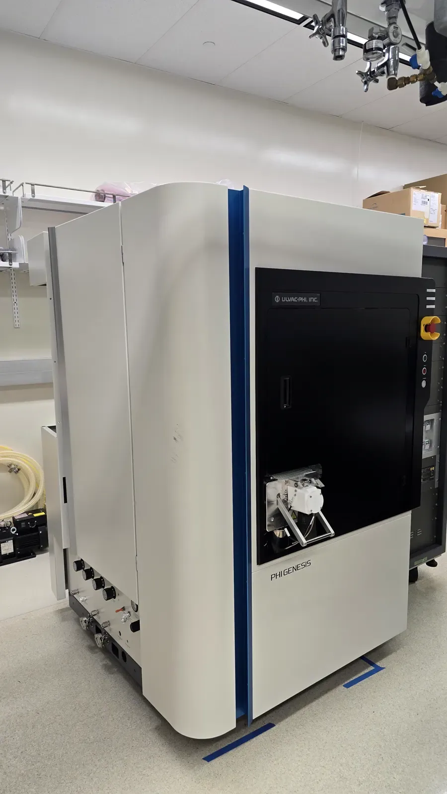
PHI Genesis X-ray photoelectron spectroscopy instrument

X-ray photoelectron spectroscopy

Surface-sensitive chemical and electronic-state analysis with the PHI Genesis XPS.

Campus Facilities

Shared UC San Diego Research Infrastructure

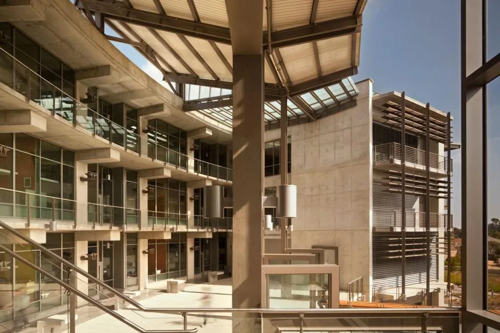
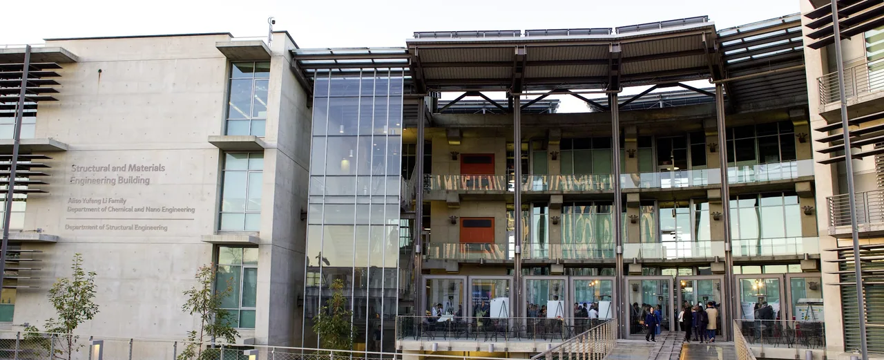
Courtyard of UC San Diego’s Structural and Materials Engineering building, home of the Materials Research Center01
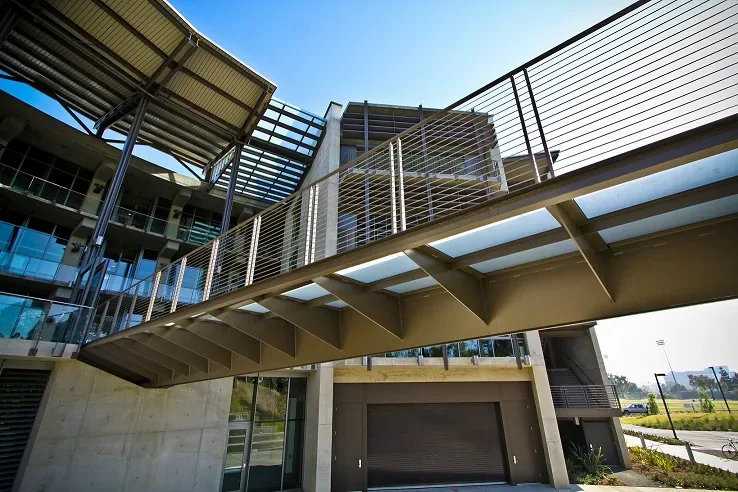
Skybridge and laboratory wing of the Structural and Materials Engineering building at UC San Diego

Structural and Materials Engineering Building

The Structural and Materials Engineering building houses UC San Diego’s Department of Chemical and NanoEngineering. Its basement laboratories put diffraction, optical spectroscopy, and scanning-probe tools a short walk from the group’s own synthesis and processing benches.
  • X-ray diffraction
  • UV-visible and FTIR spectroscopy
  • Raman and micro-photoluminescence
  • SEM
  • Accelerated Stress Testing and Device Measurement
Explore the NE-MRC
Placeholder photo for Franklin Antonio Hall — real photo to be added through the CMS02
Placeholder photo for Franklin Antonio Hall — real photo to be added through the CMS

Franklin Antonio Hall

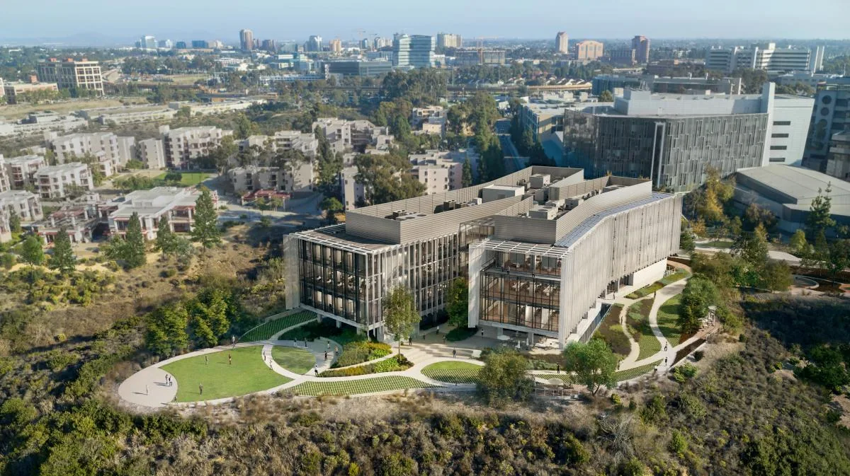
Franklin Antonio Hall is the newest building in UC San Diego’s Jacobs School of Engineering with a spacious 189,000 square feet organized around interdisciplinary “research neighborhoods” that pair theory with experiment under one roof. Named for Qualcomm co-founder and UC San Diego alumnus Franklin Antonio, it combines shared research space with active-learning classrooms and industry interaction space the group taps for collaborative projects and teaching.
  • Collaborative research neighborhoods
  • Shared instrumentation space
  • Active-learning classrooms
  • Industry interaction space
About Franklin Antonio Hall

MRSEC

The UC San Diego Materials Research Science and Engineering Center (MRSEC) is a National Science Foundation-funded hub, run jointly by the Jacobs School of Engineering and the School of Physical Sciences, that brings physicists, chemists, and engineers together around quantum and atomically tailored materials. Its Materials Characterization Facility gives the group access and training on electron microscopy and spectroscopy tools, and shared-facility partnerships with SDNI and SDSC extend that reach from nanofabrication to supercomputing.
  • S/TEM electron microscopy
  • X-ray diffraction
  • Raman, FTIR, and photoluminescence
  • Soft-matter characterization
  • SDSC computing and science gateways
Visit the MRSEC
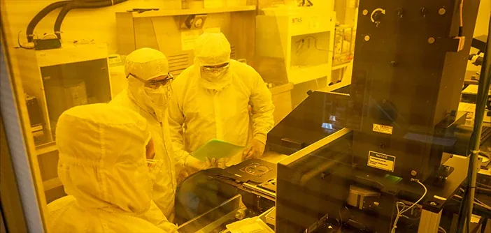
Researchers in cleanroom suits working at lithography tools in the Nano3 facility at UC San Diego04
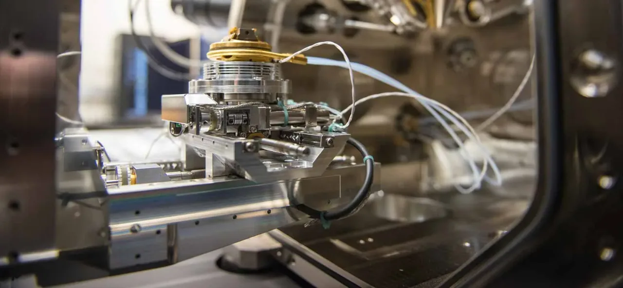
Sample stage inside Nano3’s dual-beam focused-ion-beam microscope

Nano3

Nano3 is UC San Diego’s nanofabrication cleanroom in Atkinson Hall at the Qualcomm Institute — more than 7,000 square feet of Class 100 and Class 1000 space, plus a characterization suite used by hundreds of campus and industry groups. The Fenning group relies on it for lithography, thin-film deposition, and electron-beam imaging that go beyond what fits in a single lab.
  • Class 100 / 1000 cleanroom
  • Photolithography and e-beam lithography
  • ALD, CVD, sputtering, and evaporation
  • SEM / EDS and EBIC
  • Cryogenic dual-beam FIB
Visit Nano3